What is the correct answer to the p-n junction diode NEET 2026 question?
Option C is correct: D3 has the widest depletion region, D2 the intermediate width, and D1 the narrowest. The p-n junction diode NEET 2026 question turns on one distinction: zero external bias does not remove a junction’s depletion region.
This single-correct question is from NEET UG 2026, held on 21 June 2026, Code-50, Physics, Electronic Devices. “Medium difficulty” is the question bank’s classification, not an official difficulty rating.
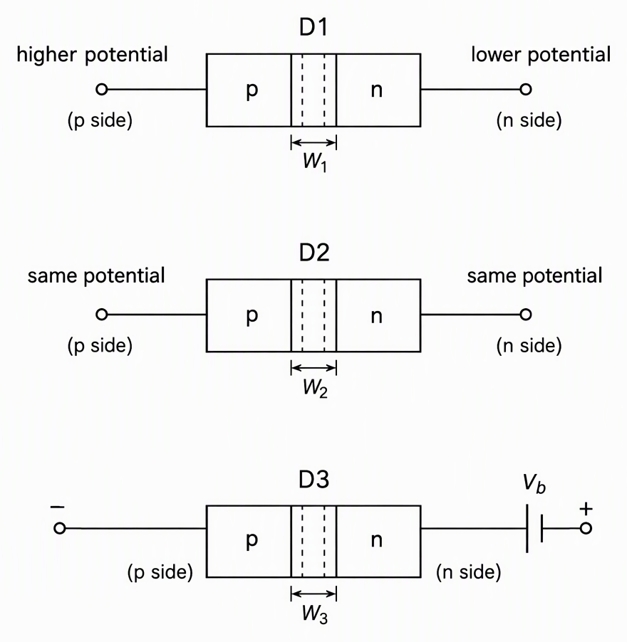
The task is to compare the depletion-layer widths of three identical junction diodes connected in a battery circuit. The original circuit image is not supplied here, so the illustration shows the bias states stated in the supplied official solution, not a reconstruction of the original wiring.
The four options are:
How do you determine the bias of each diode?
Compare the p-side terminal potential with the n-side terminal potential of that particular junction. A battery elsewhere in the circuit does not, by itself, make the junction reverse biased. Bias depends on the voltage across its own two terminals, not its position on the page.
Define the externally applied junction voltage as:
A positive value means forward bias, zero means no applied bias, and a negative value means reverse bias. This terminal voltage is separate from the built-in potential inside the junction.
The supplied official solution gives these circuit-specific assignments:
- D1: p-side potential higher than n-side potential; forward biased; depletion width decreases relative to an identical unbiased junction.
- D2: equal terminal potentials; zero net external bias; depletion width remains at its equilibrium value.
- D3: p-side potential lower than n-side potential by the full battery voltage; reverse biased; depletion width increases.
These assignments come from the supplied solution, not from tracing the explanatory panels. Without the original image, we cannot independently verify the wiring that makes D2 unbiased or assign a forward-voltage magnitude to D1.
How do barrier heights give the depletion-width order?
Reverse bias gives D3 the largest effective barrier; forward bias gives D1 the smallest. For identical junctions under the same conditions, depletion width increases with the square root of that barrier. No numerical battery voltage is needed to compare the widths.
NCERT Class 12 Physics, Chapter 14, section 14.3 gives the rule: forward bias narrows the depletion region; reverse bias widens it. Use the supplied solution’s barrier-height method, not assumptions about current.
Let the built-in potential and unbiased depletion width be, respectively:
The Poisson-derived relation uses a common positive material and doping factor because the junctions are identical:
D1 is forward biased. Its positive forward voltage reduces the effective barrier. Within the depletion approximation used here:
D2 has zero external bias. Its built-in barrier remains:
D3 is reverse biased by the full battery voltage. Define the positive battery-voltage magnitude and write its width:
The complete barrier-height chain is:
Taking square roots and multiplying by the same positive factor preserves the ordering:
Correct option: C. D2 lies between the forward-biased and reverse-biased junctions.
Zero applied bias means equal external terminal potentials, not zero built-in potential or zero depletion width. At equilibrium, diffusion leaves fixed ionised dopants near the junction; their electric field supports a depletion region without an external voltage.
How does reversing the polarity reading produce option A?
Incorrectly labelling D1 reverse biased and D3 forward biased, while keeping D2 unbiased, produces option A. Applying the depletion-width rule to those incorrect labels gives:
This is a terminal-polarity identification error, not necessarily a failure to remember the width rule. The rule can be applied correctly to incorrect bias labels.
Use this check before assigning bias:
- Locate the p/anode and n/cathode sides.
- Recognise that the diode-symbol bar denotes the cathode.
- Compare the p-side potential with the n-side potential.
A correct response earns four marks; an incorrect response earns minus one. Changing C to A therefore lowers the score by:
Which three related questions test the same method?
Test barrier comparison, equilibrium depletion and unequal reverse biases separately. These are original related practice questions, not verified past-paper questions. Solve each before reading its worked answer, using the same barrier-height method.
- Three identical junctions are forward biased, unbiased and reverse biased respectively. Rank their effective barrier heights and depletion widths.
Forward bias subtracts from the built-in barrier; reverse bias adds to it. For positive applied-bias magnitudes within the stated model:
The common positive factor and square-root relation give:
Both rankings are reverse, then unbiased, then forward, from largest to smallest.
- Both terminals of a junction are held at the same potential. Is its depletion region absent?
No. Equal terminal potentials mean zero external bias, but the built-in barrier and equilibrium depletion region remain:
“Unbiased” does not mean “no junction electric field.”
- Two identical reverse-biased junctions have the following reverse-voltage magnitudes. Which has the larger depletion width?
Junction a has the larger effective barrier and therefore the larger depletion width. Dividing their square-root width expressions cancels the common factor:
For your next circuit question, verify the original figure before assigning terminal polarities: Free NEET PYQs: Verify Papers, Keys and Chapterwise Sets.
Frequently asked questions
What is the correct answer to the p-n junction diode NEET 2026 question?
Option C is correct: W3 > W2 > W1. The supplied official solution identifies D3 as reverse biased, D2 as unbiased and D1 as forward biased. For identical junctions under the stated model, these bias states give the widest, intermediate and narrowest depletion regions respectively.
How do I identify forward and reverse bias in a diode circuit?
Compare the p-side terminal potential with the n-side terminal potential of that junction. A higher p-side potential means forward bias, a lower p-side potential means reverse bias, and equal potentials mean zero external bias. The bar in the diode symbol marks the cathode, or n side.
Does a diode have a depletion region at zero bias?
Yes, an unbiased p-n junction retains its equilibrium depletion region and built-in barrier. Diffusion leaves fixed ionised dopants near the junction, whose electric field supports this region. Equal external terminal potentials do not mean zero built-in potential.
Why does reverse bias increase depletion width?
Reverse bias increases the effective barrier across the junction. Within the depletion approximation, depletion width is proportional to the square root of that barrier, so increasing reverse bias widens the depletion region. For identical junctions, the one with the larger reverse-voltage magnitude has the larger depletion width.